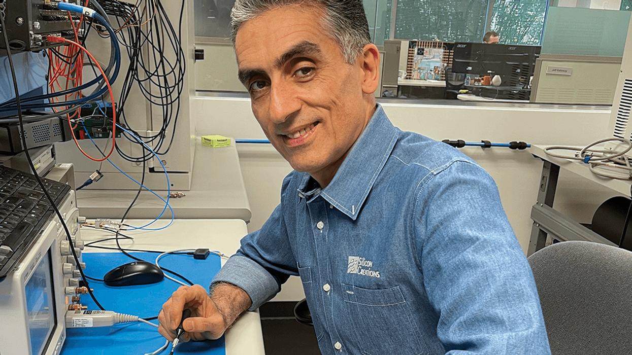
A long‑time application‑specific IC (ASIC) designer who advanced from graduate student to full professor and moved into industry in 2019 reports that modern chip design is dominated by reusable silicon intellectual property: as much as 80% of the physical area in today’s most advanced chips is occupied by blocks not designed for any single end product. That concentration of standard IP shifts engineering focus away from novelty toward getting complex, composite designs to work reliably in production — favoring engineers who can prioritize manufacturability, reuse and first‑time silicon success.
In commercial practice companies supply and integrate prebuilt silicon IP from established vendors such as Arm, Cadence, Rambus and Synopsys, alongside smaller specialists; the author joined Silicon Creations. Production designs must meet specifications consistently, yield in manufacturing and adhere to shipping schedules, so industry development flows emphasize conservative margins, extensive validation and reuse of proven blocks to reduce risk.
The premium on avoiding rework is acute because the cost of errors at advanced nodes is high: lithography masks can cost tens of millions of dollars, and a failed tape‑out can delay product schedules and revenues. As a result, teams prize first‑time silicon success and build processes that trade experimental risk for predictable outcomes and tight schedules.
Market forces are pushing more teams toward ASIC development. Demand from automotive applications and AI workloads is rising; one market estimate projects the ASIC market to grow from US $23.4 billion to $38.8 billion by 2033, while the semiconductor industry overall is projected to reach about $1 trillion by 2030. Parallel technology shifts — FinFET adoption in the mid‑2010s and the emergence of modular chiplets — have increased design complexity and raised development costs by almost an order of magnitude.
The author highlights a widening practical gap between academic research and industrial practice. Academia’s objective is to explore what’s possible — novel circuits, unconventional architectures and new knowledge — whereas industry must exploit those ideas and determine what is viable at scale. “Academia explores the design space, asking what is possible, while industry exploits it, determining what is viable at scale.
Some programs attempt to bridge the divide: Taiwan Semiconductor Manufacturing Co.’s University FinFET Program and government‑funded chip‑design hubs now allow a subset of well‑resourced universities to design for advanced architectures. Even so, the author warns that many academic groups still cannot access the current nodes, and that engineers moving into industry typically need new skills and a risk‑averse mindset that prioritizes manufacturing readiness, reuse and schedule over novelty.
Sources
Replies (0)
No replies in this topic yet.