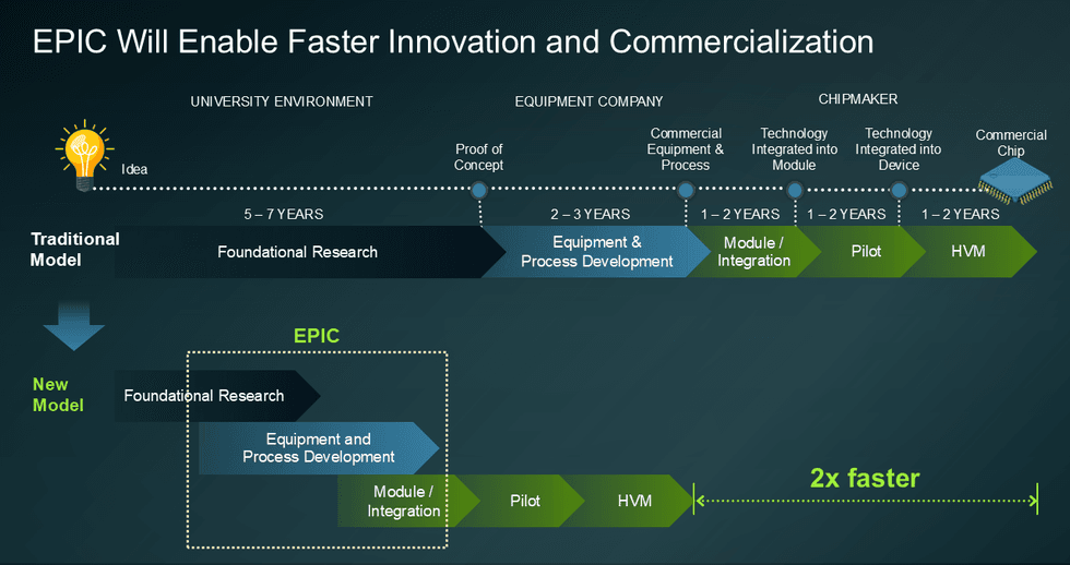
Applied Materials has committed roughly $5 billion to an EPIC center intended to accelerate advanced semiconductor equipment research and development. The company positions that investment as the largest commitment to advanced semiconductor equipment R&D in U.S. history and frames EPIC as a platform for higher‑velocity co‑innovation across the industry. EPIC is presented as a center and common platform to concentrate talent, share critical infrastructure and collapse long feedback loops that the company says are required to meet angstrom‑era challenges. The initiative emphasizes joint development of tools, processes and integration capabilities rather than sequential handoffs between isolated groups.
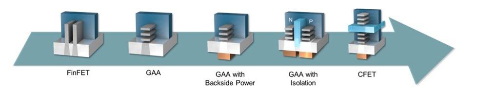
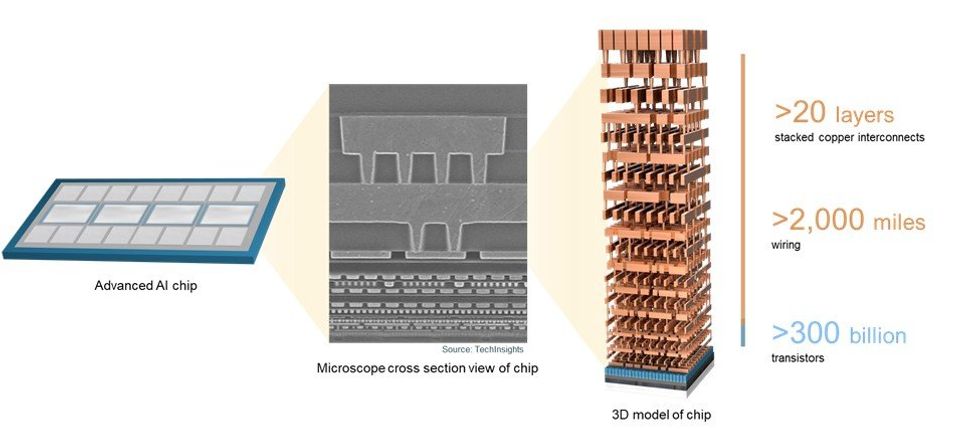
The company frames the technical challenge around three tightly coupled domains: logic, memory and advanced packaging. For logic, efficiency depends on transistor switching, low‑loss power and dense wiring stacks; memory faces surging bandwidth and capacity demands that expose a widening memory wall; and packaging must deliver 3D integration, chiplet architectures and high‑density interconnects to bring compute and memory closer.
Applied Materials argues the traditional R&D workflow — likened to a relay race of sequential handoffs — is too slow for today’s AI timelines. At angstrom scales the physics couples materials, integration, design rules, power delivery, wiring and thermal budgets, and the company warns architects cannot wait 10–15 years for successive technology inflections to mature. A central technical driver cited is energy per bit: as AI workloads scale, moving data increasingly consumes as much or more energy than raw compute. That shifts optimization from peak compute alone to system‑level designs where reducing energy per bit and improving memory proximity can extend overall performance within thermal and mechanical constraints.
Applied Materials says a long‑term perspective is essential to align materials innovation with emerging device architectures. Working with customers, the company aims to chart roadmaps across the next three to four generations and as far as ten years, using EPIC to break down silos, compress learning loops and accelerate co‑development of front‑end fabrication and back‑end integration processes.
Sources
Replies (0)
No replies in this topic yet.