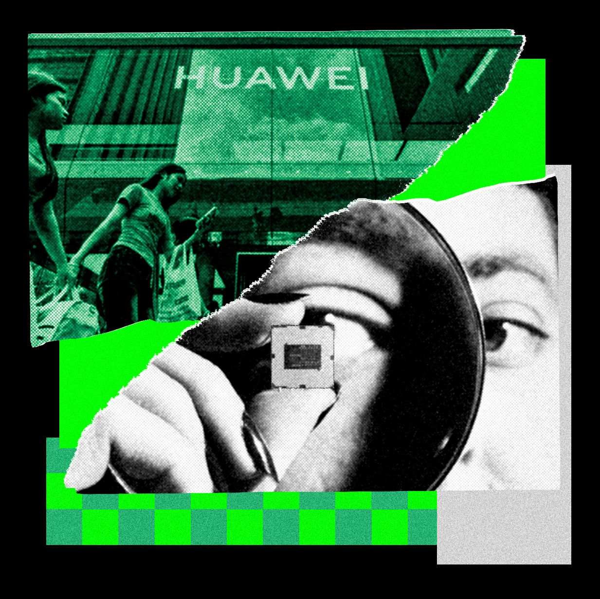
Tingbo He, president of Huawei’s chip‑design arm HiSilicon and widely known in China as the company’s “chip queen,” told the IEEE International Symposium on Circuits and Systems in Shanghai that her engineers have developed a system‑level scaling strategy called Tau’s Scaling Law. She said, “We found a new path,” and promised HiSilicon would “bring the surprise” with a demonstration in the coming months, explicitly stating it will arrive before winter 2026. The announcement frames Tau as an effort to circumvent the limits now constraining transistor shrinkage and to change how overall performance gains are pursued.
He described Tau as a shift away from pure geometric transistor scaling toward speeding computation across chips, circuits and whole systems. HiSilicon outlined concrete techniques under the Tau umbrella: LogicFolding, which reduces time for key logical operations; accounting for nanoscale electronic phenomena; co‑designing chips to operate together; and building faster interconnects to shorten chip‑to‑chip communication latency. The emphasis is on system co‑ordination rather than single‑die density.
HiSilicon positioned Tau against the backdrop of Moore’s Law hitting physical and quantum hurdles at a few nanometers. The company noted that industry players already use multi‑chip stitching to boost performance — conference remarks cited Apple’s processors as an example — and stressed that system approaches are gaining traction. At the same time, U.S. export controls bar Huawei from using TSMC’s most advanced processes, forcing reliance on China’s SMIC and older lithography tooling and contributing to an estimated multi‑year lag behind the global leading edge.
HiSilicon’s timeline is explicit: it says components built under the Tau approach could reach performance equivalent to a 1.4‑nanometer process by 2031, while TSMC is expected to introduce commercial 1.4‑nm chips closer to 2028. He framed Tau not as incremental work but as “a big leap ahead,” while acknowledging that the company must still prove the approach’s viability amid sanctions and tooling limits.
Observers and analysts urged caution. Some argue export controls have pressured Huawei to pursue system‑level innovation that could, over time, narrow China’s chipmaking gap and have strategic consequences for U.S. technological advantage. Independent analyst Lennart Heim said Huawei’s strategy indicates the company is confronting limits on how much further performance can be squeezed from traditional shrink‑and‑densify tactics, highlighting uncertainty about whether system techniques can fully compensate.
For builders and AI teams the practical takeaway is concrete: HiSilicon stresses that performance wins for both training and inference rely on shortening the time data spends moving, not only on raw compute clocks. If LogicFolding, improved interconnects and chip co‑design deliver as claimed, system architects will need to prioritize inter‑chip latency, data locality and hardware‑software co‑optimization — while supply‑chain constraints around lithography and foundry access remain a gating factor.
Sources
Replies (0)
No replies in this topic yet.